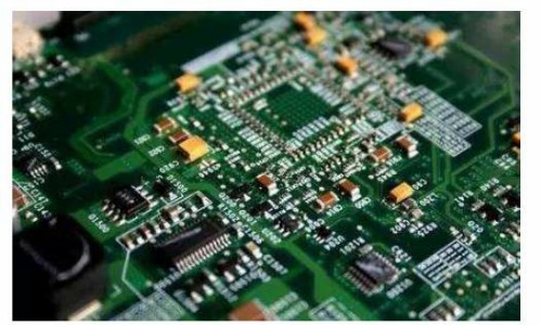
In any switching power supply design, physical design of PCB is the last link, if the design method is unpropriate, PCB may produce too much radiation, electromagnetic interference caused by unstable power supply working, aiming at the matters needed attention in the steps below are analyzed:
1# From the schematic diagram to the PCB design process
- > element parameters input principle of network design parameters table - > Settings - > manual layout - > the manual wiring - design - > > validation review - > CAM output.
2# Parameters set
Adjacent wire spacing must be able to meet the requirements of electrical safety, and to facilitate the operation and production, also should try to wide spacing. Minimum spacing can be suitable to withstand voltage, in wiring density is lower, the line spacing can be appropriately increased, the high and low level disparity of signal lines should be as much as possible short and increasing spacing, line spacing will generally set to 8 mil. Welding disc hole edge to the distance from the edge of the PCB is greater than 1 mm, so that you can avoid solder defects due to process. When connected to the welding plate is fine, get the line to connect between the pads and go line design into water droplets, such are the benefits of bonding pad is not easy to peel, but go line and welding plate is not easy to disconnect.
3# Components layout
Practice has proved that even if the circuit principle diagram design is correct, improper printed circuit board design, can produce adverse effect on the reliability of electronic equipment as well. For example, if the two parallel lines in close proximity, PCB will form the signal delay, reflection noise in transmission line terminal formation; Due to switching power supply, the ground wire is not consideratable, make the product performance degradation, therefore, in the design of printed circuit boards, should pay attention to the right way. there are four current loop in each switching power supply,
1. The switching power supply ac circuits
2. The output rectifier ac circuits
3. The input signal source current loop
4. The output load current loop input circuit through an approximation of the dc current of input capacitance charging
The best way to build switching power supply layout and its similar electrical design, optimal design process as follows:
1. Place the transformer
3. Design output rectifier current circuit
4. Connect to the ac power control circuit of the circuit
Design input current source circuit and the input filter design output load circuit and output filter according to the function of the circuit unit, all components of circuit layout, have to comply with the following principles:
1. The first thing to consider PCB size. PCB size is too large, the printing lines long, impedance increases, the ability to resist noise down, cost also increase; heat dissipation is too small to good, and the adjacent lines are susceptible to interference. Circuit board is the best shape of rectangular, aspect ratio is 3:2 or 4:3, located in the edge of the circuit board components, circuit board edge is generally not less than 2 mm.
2. To consider when placing device after welding, don't be too dense.
3. For the center with the core of each functional circuit components, layout around it. Compact components should be even and neat arranged on the PCB, as far as possible to reduce and shorten the lead and the connection between the components, VCC decoupling capacitor close to the device.
4. Working under high frequency circuit, have to consider the distribution of components between parameters. General circuit should be as far as possible make components parallel arrangement. In this way, not only beautiful and easy fabrication, but also easy to mass production.
5. According to the process of the circuit to arrange the location of each functional circuit unit, to facilitate signal flow, layout and make the signal as much as possible to maintain consistent direction.
6. The layout of the first principle is to ensure that the wiring of the completion rate, attention to fly line connection when mobile device, the device together with attachment relation.
7. As much as possible to reduce the loop area, and to inhibit the radiated interference of switching power supply.
